
design process for PCB rigid flex work
The design process for PCB rigid flex is complex, with different fabrication steps and challenges. The process can be more costly than traditional PCBs, so it is important to plan ahead and consider all aspects of the design. The key to success is to have a well-defined and structured design, which is both cost-effective and flexible enough for the intended application.
Rigid flex PCBs combine the benefits of both rigid and flexible circuit boards. The PCBs can bend and flex to conform to the product’s shape, and they are more durable than conventional PCBs. Using these boards will increase the product’s reliability, reduce assembly time, and cut down on manufacturing costs.
A typical pcb rigid flex has two flex sections embedded within three layers of the main board. The flex section can be made of two 2-layer flex circuits, or one 2-layer and a 3-layer flex circuit. The layers in the flex section are laminated inside the main PCB stack up, which protects them from exposure to the outer layer plating and helps improve impedance control.
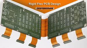
How does the design process for PCB rigid flex work?
This design is also more efficient than having a single rigid board with a separate flex section. The extra layers in the flex area can reduce signal loss and reduce power delivery problems caused by thermal expansion. In addition, the flex section can be made thinner to save on material and component costs.
The most important design consideration in a rigid-flex PCB is the minimum bend radius. A large enough radius will ensure that the flex section doesn’t put too much stress on copper conductors. This will prevent the conductors from fracturing or becoming unreliable over time. A good rule of thumb is to have the flex radius six times larger than the thickness of the flex section.
There are several ways to meet the required bend radius, including using solid copper pours and hatched polygons. Both have advantages and disadvantages, but hatched polygons offer the best flexibility for this type of circuit. Hexagonal hatched polygons have particularly high flexibility, and they also provide better resistance to buckling than solid polygons.
In addition to ensuring a robust flex section, rigid-flex PCBs should have stiffeners for areas susceptible to excessive pressure. Stiffeners help to relieve strain, balance weight and heat dissipation, and they can also help to prevent stress and abrasion. The stiffeners can be made of a variety of materials, including aluminum and stainless steel. They can be attached with thermally cured acrylic adhesives or pressure-sensitive adhesives.
PCB rigid-flex technology combines rigid and flexible circuit board elements into a unified structure, providing a hybrid solution that meets the demands of various electronic applications. This technology integrates flexible circuits with rigid circuit boards, allowing for complex designs that can be bent or folded while maintaining electrical connectivity. The rigid sections provide mechanical support and structure, while the flexible segments allow for movement, which is essential in applications requiring compact, reliable connections between different components.
Once the layout design is finalized, the next step in the rigid flex manufacturing process is the component placement. Traditionally, this was done by hand, but nowadays it’s accomplished with automated pick-and-place machines. These machines are more accurate and fast than humans, which means they can get the job done quickly and efficiently.


+ There are no comments
Add yours