
printed wiring assembly handle electromagnetic interference
Printed wiring assemblies (PWAs) play a crucial role in electronic systems, but they are susceptible to electromagnetic interference (EMI), which can degrade performance and reliability. EMI refers to the disturbance of electromagnetic fields that can interfere with the operation of electronic devices or systems. To mitigate the effects of EMI and ensure the proper functioning of printed wiring assemblies, designers employ various techniques and strategies to minimize electromagnetic interference.
One of the primary methods for handling electromagnetic interference in printed wiring assembly is through proper layout and routing of signal traces. Careful attention is paid to the arrangement of traces on the printed circuit board (PCB) to minimize the coupling of electromagnetic fields between adjacent traces. Signal traces carrying high-speed or sensitive signals are routed with sufficient spacing between them and with minimal crossing to reduce the likelihood of crosstalk and interference. Additionally, signal traces may be routed in differential pairs or shielded with ground planes or guard traces to further attenuate EMI.
Another effective technique for mitigating electromagnetic interference in printed wiring assemblies is the use of shielding. Shielding involves enclosing sensitive components or circuits within conductive enclosures or shields to block external electromagnetic fields. Shielding can be implemented at the PCB level using grounded copper planes or at the component level using metal enclosures or shielding cans. By preventing external electromagnetic fields from reaching sensitive components, shielding helps maintain signal integrity and reduce the risk of EMI-induced errors or malfunctions.
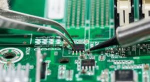
How do printed wiring assembly handle electromagnetic interference?
Furthermore, the selection of components and materials can also influence the susceptibility of printed wiring assemblies to electromagnetic interference. Components with built-in EMI filtering or suppression capabilities, such as ferrite beads, capacitors, and inductors, can help attenuate unwanted electromagnetic noise and improve the overall electromagnetic compatibility (EMC) of the assembly. Similarly, using materials with low dielectric constants and loss tangents can minimize signal attenuation and distortion caused by EMI.
Grounding and bonding techniques are essential for managing electromagnetic interference in printed wiring assemblies. Proper grounding ensures that electrical signals have a clear return path and that electromagnetic fields are effectively dissipated to ground. Ground planes and traces are strategically placed on the PCB to provide low-impedance paths for return currents and to minimize ground loops, which can exacerbate EMI issues. Bonding refers to the physical and electrical connection of metallic components and enclosures to create a continuous conductive path for EMI mitigation. By establishing a robust grounding and bonding scheme, designers can minimize the impact of electromagnetic interference on printed wiring assemblies.
In addition to proactive measures, printed wiring assemblies may also undergo testing and validation procedures to assess their electromagnetic compatibility and susceptibility to interference. Electromagnetic compatibility (EMC) testing involves subjecting the assembly to various electromagnetic fields and assessing its performance and emissions levels. By identifying potential sources of interference and evaluating the effectiveness of mitigation measures, EMC testing helps ensure that printed wiring assemblies meet regulatory requirements and perform reliably in real-world operating environments.
In conclusion, handling electromagnetic interference in printed wiring assemblies requires a multifaceted approach that encompasses layout optimization, shielding, component selection, grounding, bonding, and testing. By implementing these techniques and strategies, designers can minimize the effects of EMI and ensure the proper functioning and reliability of printed wiring assemblies in electronic systems. As electronic devices continue to proliferate and operate in increasingly complex electromagnetic environments, the importance of effective EMI mitigation techniques in printed wiring assembly design cannot be overstated.


+ There are no comments
Add yours