
Printed Circuit Board Assemblies
Grounding is an important element of a printed circuit board (PCB) design. It is used to ensure that electrical signals do not interfere with each other, preventing data corruption or other problems. Unfortunately, improper PCB grounding can degrade performance and reliability.
There are several different ways to ground a printed circuit board assemblies, and different techniques will work better for different types of circuits. For example, some methods are better suited for high-speed circuits than others. To avoid common grounding issues, you should always make sure to follow the best practices for your specific design.
One of the most important elements of a PCB is the ground plane, which is the large copper layer that provides a return path for current and acts as a shield to help reduce impedance. The grounding plane is normally located on the bottom layer of the PCB, but it can be placed on the top or middle layer as well.
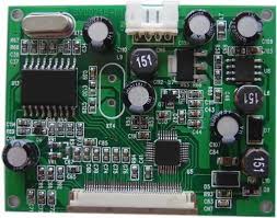
Grounding in Printed Circuit Board Assemblies
Another way to ground a circuit is through the power net, which is a set of traces that connect each component to a source of power. However, the power net can create a loop of current that may cause interference with other components. This problem is called a ground loop, and it can lead to erratic behavior in the system. The solution is to make sure that the PCB is properly sized and routed, with the power nets separated from each other as much as possible.
Some designers also use a technique known as single point grounding, which entails connecting all of the signals in a circuit to a single ground reference point. This eliminates the need to use multiple points of grounding, and it can improve signal quality. However, this method can be difficult to implement with complex designs.
There are a number of different factors that can affect the grounding of a circuit, including the voltage spikes in the power supply and crosstalk between adjacent signals. Some of these issues can be minimized by using proper sizing and routing, employing isolation techniques, and utilizing unique signal handling techniques.
The grounding of a circuit is essential for the overall function and integrity of the system. If not done correctly, it can lead to a host of problems, such as signal crossroads and spurious ground voltage. The good news is that the vast majority of these issues can be avoided by choosing the right grounding techniques.
There is a lot that goes into creating a good grounding strategy for a PCB, and it is vital to make sure that all of the mounting holes are properly grounded. While some people will argue that mounting holes should never be connected to the enclosure, this is not a universal rule and it can depend on the type of board and the specific design requirements. By following these tips, you can avoid many of the most common grounding errors in Printed circuit board assemblies. This will ensure that the system performs as intended and can be safely mounted in an enclosure.


+ There are no comments
Add yours